最大源漏极电压VdsDrain-Source Voltage| 50V
●\---|---
●最大栅源极电压Vgs(±)Gate-Source Voltage| 20V
●最大漏极电流IdDrain Current| 510mA/0.51A
●源漏极导通电阻RdsDrain-Source On-State Resistance| 4Ω@ VGS =4.5V, ID =350mA
●开启电压Vgs(th)Gate-Source Threshold Voltage| 1~2.5V
●耗散功率PdPower Dissipation| 960mW/0.96W
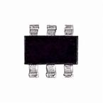
●Description & Applications| Dual N-Channel Enhancement Mode Field Effect Transistor General Description These dual N-Channel Enhancement Mode Field Effect Transistors are produced using Fairchild’s proprietary, high cell density, DMOS technology. This very high density process has been designed to minimize on-state resistance, provide rugged and reliable performance and fast switching. These device is particularly suited for low voltage, low current, switching, and power supply applications. Features • High saturation current • High density cell design for low RDS(ON) • Proprietary SOT –6 package: design using copper lead frame for superior thermal and electrical capabilities
●描述与应用| 双N沟道增强型场效应晶体管 概述 这些双N沟道增强型场效应晶体管都采用飞兆半导体专有的,高细胞密度,DMOS技术。这非常高密度工艺已旨在最大限度地减少通态电阻,提供坚固可靠的性能和快速切换。在这些设备特别适合于低电压,低电流,开关,电源中的应用。 特点 •高饱和电流 •高密度电池设计的低RDS(ON) •专有SOT-6包装设计采用铜引线框架的卓越热和电气性能


